

Posted by Henrik Kryh
Table of contents
Electromagnetic compatibility (EMC) is not just a regulatory formality but a cornerstone of product reliability and market success. In this blog post, you can learn about the benefits of running EMC simulations with CST Studio Suite electromagnetic simulation software.
You’ll also learn which file formats are supported, so that your simulation project can be setup as quickly and as accurately as possible. A switched mode power supply will be used as an example to describe the workflow of emissions simulations because it’s a subsystem commonly investigated in terms of EMC performance. However, the workflow is not subsystem specific.
Why Simulate Electromagnetic Compatibility (EMC)?
Electrical products need to comply with the EMC/EMI directives before they are allowed to be sold. This is done to make sure that your product does not cause disturbances to other electronic systems (emission requirements) but also to ensure that your device is resilient against electromagnetic interference (immunity requirements).
Compliance is typically ensured by performing a number of standardized tests at a 3rd party test house when product development is completed. Unfortunately, many products will not pass their first EMC compliance test. So instead of launching the product, it needs to be re-designed.
This is of course costly, it affects the time-to-market, and troubleshooting and re-design becomes an activity of top priority. In order to reduce the number of surprises in such a late development stage, more and more companies are now using simulation to reduce the risk of not passing their EMC tests.
Some benefits of using simulation for EMC include:
- having the opportunity to investigate your design before the first prototype is even manufactured,
- improving your product knowledge by visualizing the electromagnetic fields to see how they propagate in your product
- by using virtual prototyping, you can evaluate more design iterations compared to a conventional workflow.
Simulation helps when making comparisons of design options. Will the electromagnetic fields behave as expected, and will the noise be reduced? Check out the section called Design Iterations to learn more.
Which Software Should You Use for EMC Simulations?
Some people dismiss EMC simulations because they envision it to be too complex. However, there has been a lot of progress in EMC simulation in recent years and EMC simulations with CST Studio Suite are mature with well-established workflows.
CST Studio Suite includes full wave 3D solvers, which fully solve Maxwells equations in 3D so that you don’t have to estimate parasitic components and coupling paths within the device. There’s a wide range of import options, and PCBs can be imported from most EDA/ECAD tools using ODB++ or IPC-2581 file formats. To increase simulation speed and reduce complexity, you can choose to only import the relevant part of the PCB using e.g., area, nets, and layers selections. This allows you to simulate the different subsystems of your PCB individually.
CST also has extensive import options when it comes to 3D MCAD files, and importing from SOLIDWORKS, CATIA or other CAD software is included. When your product’s 3D geometry has been imported to CST Studio Suite, it’s time to add the circuitry to the schematic view of your simulation project.
It’s not recommended to include all components of PCB. Just include those that will affect the functionality of your selected subsystem. Component models can be imported as e.g., SPICE, IBIS, or Touchstone files.
In EMC testing, you power up your device, and you get a pass or fail result. When working with simulations, the recommendation is to select a subsystem which you’d like to investigate. While this might seem like a needle-in-a-haystack problem, most designers have a good understanding of their product and know which subsystems have the highest risk of not passing the EMC test.
While there are multiple possibilities in terms of what EMC simulation to run first, simulations of conducted emissions are a great starting point.
Simulation of Conducted Emissions
Many systems contain Switched Mode Power Supplies, SMPS, which are known for generating noise, and because of this they are one of the usual suspects in EMC compliance failures. The functional schematic of a SMPS, a DC-DC Buck Converter, and its corresponding PCB is shown in figure 1.
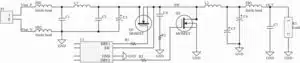
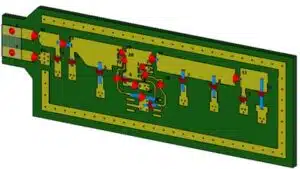
Figure 1. Schematic and PCB of a Buck Converter used for EMC Simulation
The input voltage Vbat is 12 V and the output voltage is 5 V. The red cones on the PCB represents ports, which are used in CST to couple the 3D model to the schematic. In figure 2, the schematic view of the CST simulation project is shown. As can be seen, each port in the 3D model is represented by a pin on the 3D block in the schematic. These pins are used to connect component models to the 3D model.
In this example, all components are represented by SPICE models. Only one component is missing compared to the functional schematic in figure 1, and that is the MOSFET driver, U1. Instead, the drive signals to R1 and R5 are defined by complementary time signals, defined by the min and max voltage, rise and fall times, duty cycle and time period/switching frequency.
At the bottom of the schematic, the Line Impedance Stabilization Network (LISN) is connected, to resemble the measurement setup. Present in the schematic are also numerous probes to be able to monitor voltages and currents at different nodes.
The use of the ground symbol in the schematic below might seem a bit odd, but the schematic is set up correctly for use in CST Studio Suite.
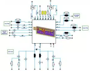
Figure 2. The Schematic View of the simulation project in CST
Before running the simulation, the frequency range of the simulation need to be specified. In this case, the solver is set up to run from 0 to 300 MHz. This is to make sure that the harmonics of the SMPS can be seen in the simulation. In figure 3 the drive signals, the input and output voltage as well as the voltage on the LISN-P node is displayed.
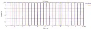
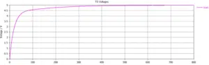
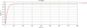
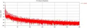
Figure 3. A selection of different voltages in the buck converter simulation project
In the animated picture below, you can see the H-Field of the PCB at 1.25 MHz, which is the switching frequency of the drive signals.

Simulation of Radiated Emissions
The setup of Radiated Emissions simulations is very similar to the setup of Conducted Emissions simulations. The PCB is imported in the same way, and the schematic need to be setup in the same way with component models and drive signals – but typically the frequency range is increased.
The next step would be to add field probes to the 3D view to record the electric field. With the click of a button, you can add a sphere of probes to capture the fields around your device, as can be seen in figure 5.
When performing EMC measurements, the device is measured with an antenna at a fixed position, and then the device is rotated, to make sure that the device is compliant with the requirements in all directions. By using the setup with the sphere of probes, the radiation in all directions can be found in a single simulation to save time.
In EMC measurements we’re typically provided with the worst case values, and using a post-processing macro in CST, also just by the click of a button, we can get the worst case values by using the envelope of all the probes, as can be seen in figure 6.
CST also offers the possibility to include limit lines in plots. Limit lines from some well-known standards are included, but the user also has the possibility to define their own limit lines, which makes it easy to visualize e.g., internal requirements as well.

Figure 5. A sphere of probes is set up to capture the radiated emissions from the PCB
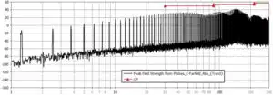
Figure 6. The envelope of the radiated emissions from all probes, plotted in black. Limit lines for quasi-peak in red.
Design Iterations
When your simulation is properly set up, you can easily create design iterations and perform what-if-analyses, just like you approach them in the measurement lab. You can check the impact of component changes, and you can see what happens if you insert a filter on your PCB.
Some of these changes can be done as easily as in the measurement lab. But other changes, like evaluating changes to a reference plane inside a PCB, are more conveniently done using simulations. By visualizing the fields, you also get an understanding of what’s happening on your PCB, rather than simply discovering that your latest change resulted in a 3dB improvement.
Get Started with EMC Simulation
Conducted and radiated emissions are a great starting point for EMC simulations. However, there are many established workflows for EMC simulations and CST Studio Suite comes with a component library with ready-to-run simulation examples. A few examples include DC-DC-converters, an inverter, a bulk current injection probe, an ESD example and a shielding effectiveness demonstration. CST also comes with Project Templates to help you set up your simulation project correctly in terms of boundary conditions, mesh settings, probes etc.
Let us know if you need support with onboarding to speed up the learning process, or if you’re interested in attending a full-day training course on how to use CST for EMC simulations.

TECHNIA Simulation provides top tier FEA, Non-linear, and Advanced Simulation Software, Training, and Consultancy. Our dedicated team of more than 65 Simulation experts across 16 countries advise and support your innovation with a wealth of specialist knowledge and experience.
About TECHNIA- Related news and articles straight to your inbox
- Hints, tips & how-tos
- Thought leadership articles
Helping you find the information you’re looking for. Discover webinars, events, FAQ's, case studies and tutorials.
VIEW HUB